Linksys WRT54G/WRT54GS Dual Serial Port Mod
This page contains instructions on how to add two serial ports (one
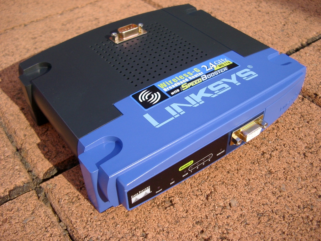
DB9 Female DCE port and one DB9 Male DTE port) to a Linksys WRT54G
(version 2 hardware) or Linksys WRT54GS wireless router.
THIS WILL VOID THE WARRANTY ON YOUR ROUTER.
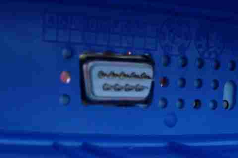
The DB9F (Female) connector on the front is wired as a DCE (think
of this as a peripheral serial port), and can be connected directly to
the serial port on a host PC. This gives you access to the built-in
serial console on the router (115200, 8, N, 1).
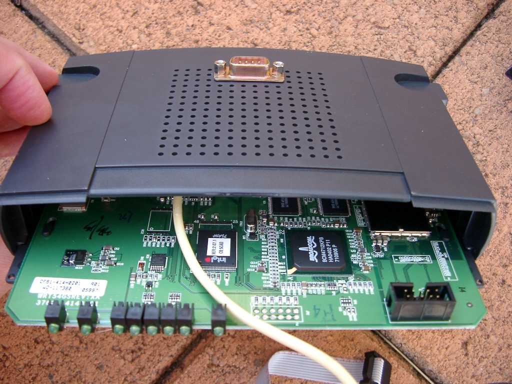
The DB9M (Male) connector on the top is wired as a DTE (think of
this as a host serial port), and can be connected directly to
peripherals like an external serial modem, or other serial devices
which are normally connected to the serial port on a host PC.
The pinout of JP1 on the Linksys PCB is as follows:
Pin  1: 3.3V        Pin  2: 3.3V
Pin  3: Tx (ttyS1)  Pin  4: Tx (ttyS0)
Pin  5: Rx (ttyS1)  Pin  6: Rx (ttyS0)
Pin  7: NC          Pin  8: NC
Pin  9: GND         Pin 10: GND
Note that neither of the serial ports support hardware flow control
(it's not pinned out on JP1 on the Linksys PCB), so you need to use
software flow control when connecting to these ports.

Requirements
Remember, this will void the warranty on your router. I
take no responsibility for your actions.
Instructions
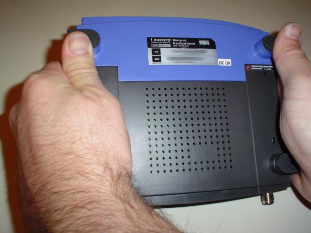
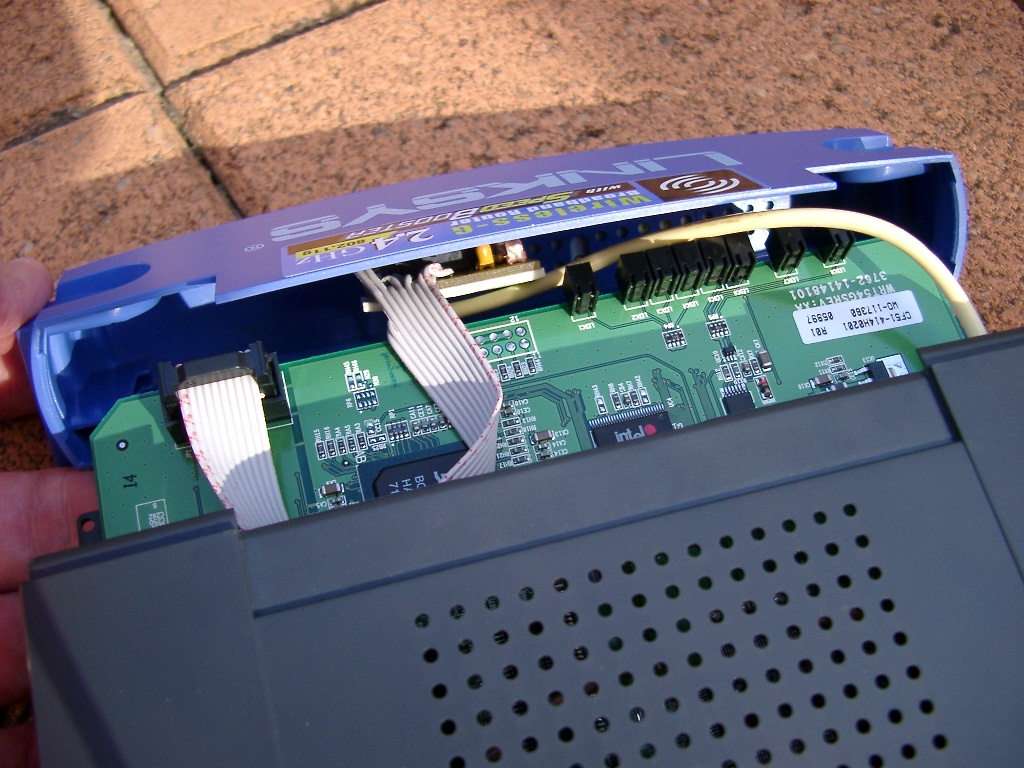
- Open up your wireless router. This step will void
the warranty on your router. I used Void Main's instructions
(the picture is linked from his site, and those are his hands,
not mine).

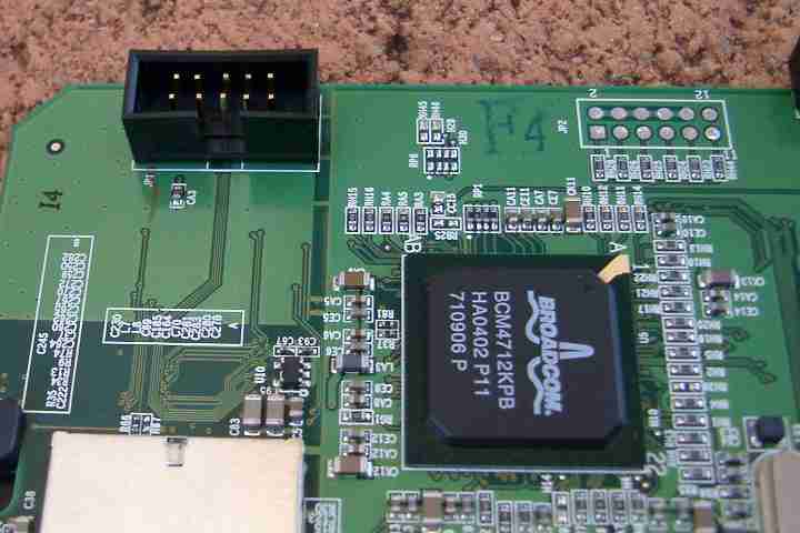
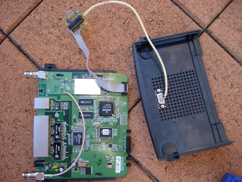
- Solder the 10 pin IDC male PCB-mount header at JP1 on the
board, as shown below. This step will *really* void the
warranty on your router. This is the only soldering you
need to do on the Linksys PCB. You might like to re-assemble
your router and test it out just to check that it still works
after this step.

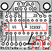
- Build up the AD233BK kit as per the instructions provided
with the kit, with the following modifications:
- Do not solder on the four pin header for J1 and J2.
- Cut the track between the left-hand pin of J1 and pin 7 of the DB9F connector
(the right-hand pin of J1 will be used for the second serial port).
- Cut the track between the right-hand pin of J2 and pin 8 of the DB9F connector
(the left-hand pin of J2 will be used for the second serial port).
- Do not solder on the two pin header for J3 (it will always be shorted,
so just solder a wire across the two pins for J3).

-
You can either solder the included DB9F PCB-mount connector
onto the board (and mount that to the front of the case), or
do as I did and extend the connections using wires to allow a
new DB9F connector (the kind which is normally connected to
the end of a cable instead of mounted on a PCB) to be mounted
through the front of the case with the metal plate on the
front covering the ugly hole.
I found the best spot to mount this connector is right
where it says "Wireless-G Broadband Router" on the front of
the case. Use the holes in the case a a guide (they line up
exactly with the mounting holes for the DB9F connector)
I left the connections between the AD233BK PCB and the DB9F
connector to last (just before closing up the case), and it
was a bit tricky but worth the effort to get a good looking
finish.

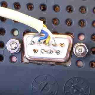
- The wires for the second serial DB9M connector are soldered
to the right-hand pin of J1 (RXD - the white wire in the picture
below), the left-hand pin of J2 (TXD - the yellow wire in the
picture below) and GND (I used the grey wire which you can't see
under the white and yellow wires, and connected it through
left-hand pin of J1 and then shorted it to GND on the underside
of the PCB). The blue wire which you can see in the picture is
not connected to anything in particular (I tied it off using the
right-hand pin of J2).


The second serial DB9M connector (which I mounted on the top
of the case) is connected to the other end of the wires as
follows:
- Connect RXD (right-hand pin of J1, the white wire in the
picture) to pin 2.
- Connect TXD (left-hand pin of J2, the yellow wire in the
picture) to pin 3.
- Connect GND (the grey wire in the picture) to pin
5.
- Connect pins 7 and 8 together on the DB9M connector
(this is the RTS/CTS handshake). You can plainly see this on
the picture.
- Connect pins 4 and 6 together on the DB9M connector
(this is the DTR/DSR handshake). This is a bit harder to see
on the picture, but I assure you it's there.
- If you're wondering what the blue wire connected to pin
4 is all about, well just ignore it and pretend it isn't
there. It's not connected to anything at the other end, so
you don't need it.
- Pins 1 and 9 are not connected to anything.

-
Crimp some cable into the 10 pin IDC female cable-mount header
(make sure the wire marked in red is orientated to pin 1 which
is normally marked with an arrow), and wire it to the AD233BK
PCB as follows:
- Connect
wires 1 and 2 (both VCC) to "+5V" on the PCB. Note that the voltage
supplied by the WRT54G is 3.3V, but the MAX233 chip on the PCB can
handle both 3.3V and 5V.
- Connect wire 3 (ttyS1 TXD) to "Rt" on the PCB.
- Connect wire 4 (ttyS0 TXD) to "Tx" on the PCB.
- Connect wire 5 (ttyS1 RXD) to "Ct" on the PCB.
- Connect wire 6 (ttyS0 RXD) to "Rx" on the PCB.
- Leave wires 7 and 8 unconnected.
- Connect wires 9 and 10 (both GND) to "-" on the PCB.


-
Mount the DB9M connector on the top of the case, plug the 10
pin IDC female cable-mount header into JP1 on the Linksys PCB,
and solder the wires through the front of the case onto the
DB9F connector.


-
Double-check all connections, and then re-assemble the router case.
If you find any ambiguous or non-obvious instructions on this
page, or have any trouble at all in following the instructions,
then please let me know.
Did I mention that this will void the warranty on your
router, and that I take no responsibility for your actions? Sure I
did. Don't bother sending your legal folk my way ...
http://www.rwhitby.net/
-- Copyright © 1997-2004 --
Rod Whitby
